Capabilities
ENGINEERING:
Design
Layout
Dxf to gerber
Gerber to Dxf
Reverse engineering
Panelization
Paste File
BOARD TYPE:
Single sided
Double Sided
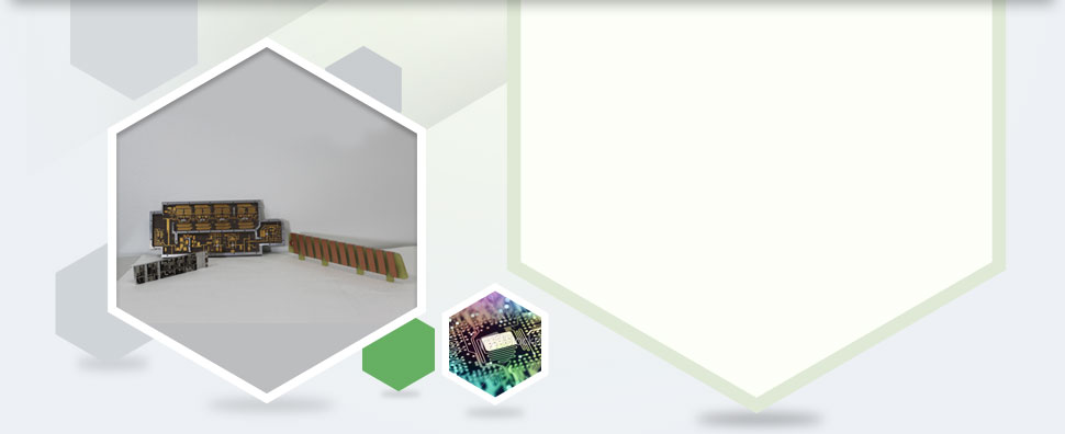
Multi-layers
Thru Holes and Surface Mount
MATERIALS:
FR4 (TG of 170/180+)
GETEK
CEM-1
CEM-3
ARLON
TACONIC
ROGERS
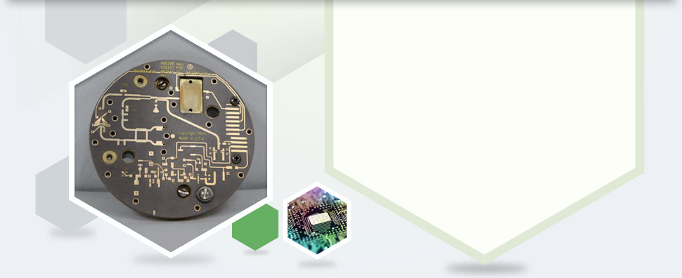
TEFLON laminate circuit boards for RF and microwave industries.
COMPOSITE multi layers
ALUMINUM backed single layers boards for LED lighting industry
CONDUCTIVE bonding of any printed circuit boards to aluminum, brass, and copper machined carriers and housings.
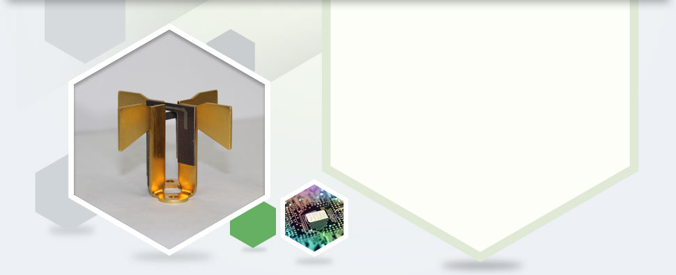
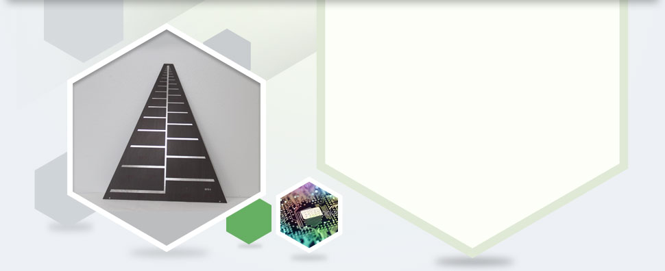
ANTENNA’s (Large communication, conical, cylindrical, conformal multi layers and geometric).
CERAMIC substrate circuitry
MATERIAL THICKNESS:
0.001 to 0.250
SPECIAL CAPABILITIES:
Board size up to 36 inches
Finished CU thickness up to 4 oz
Fine line application, width/space 005/005
Smallest hole 0.008
Mixed technology
Plated and non plated slots.
Edge plating
SOLDER MASK:
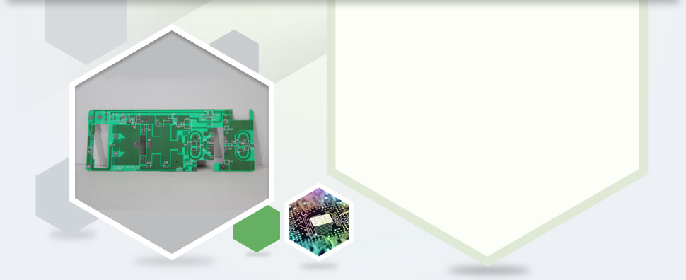
Green
Blue
Red
White
Black
Yellow
SILK SCREEN INKS:
White
Black
Red
Yellow
FINISHES:
Hot air Leveled solder (tin/lead and lead free solder)
Electroless Emmersion nickel/immersion gold
Hard gold plating
Gold tabs
White Tin
Immersion Silver.
Carbon and resistive ink.
Peelable mask
FABRICATION:
Routing
Tab routing
Scoring and Jump scoring
Panelization
Countersink and counter bore drilling
Edge Beveling
STANDARDS:
UL APPROVED
RoHS Compliant
Lead-free
100% electrical Testing(Fixture and probe)
100% In-Process Inspection
ISO 9002 QUALITY SYSTEMS SPECIFICATIONS
FINAL INSPECTION – 100% of fabricated material
Prototype Turn Around
24 HOUR


